Blog 10: Interpreting results
May 21, 2025
Hi everyone, welcome back! I kind of have been putting off interpreting my data because I wanted to learn more theory, but I have came to the conclusion that this is too hard for me and I probably need a couple more years of physics. So, I ended up relying on directly asking Dr. Smallwood and Luke (SJSU student) questions, though I tried to find what they said in papers, too. For the rest of this post, I’m going to put in data from using both the HeCd laser (fewer data points) and the HeNe laser (more data points) for peak position, width, and area, and then attempt to explain the trends.
Peak position
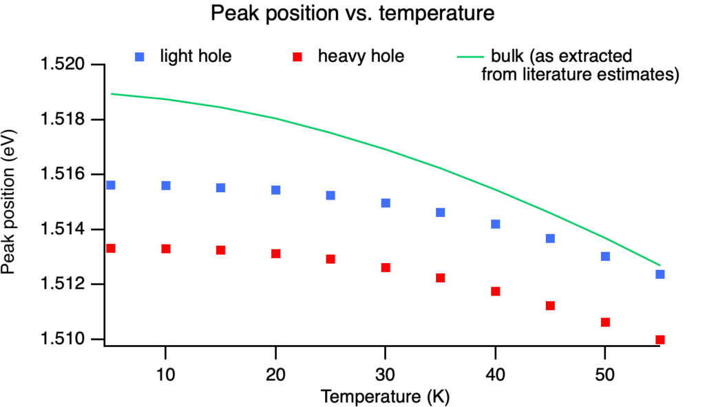
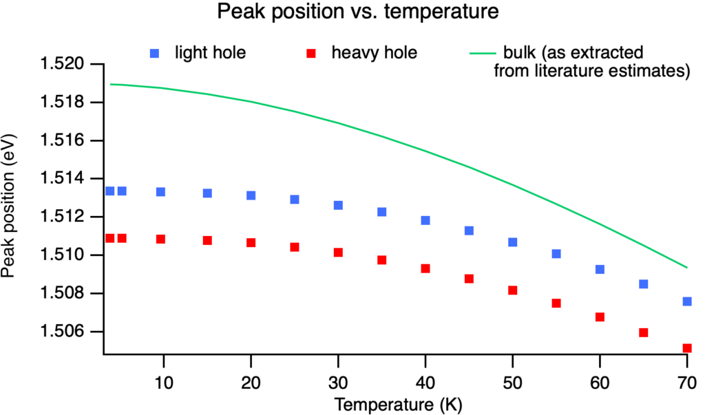
For this one, I also added a green line representing the band gap of bulk GaAs, graphing the equation from the Ioffe Institute, Eg=1.519-5.405·10-4·T2/(T+204) (eV). We can see an expected decrease in the band gap, which is very closely related to the peak position. Physically, this is because as temperature increases, atoms vibrate more, and the average interatomic distance increases. From this graph of the electronic bands in a material, we can see that the band gap decreases as the interatomic distance increases.
Peak width
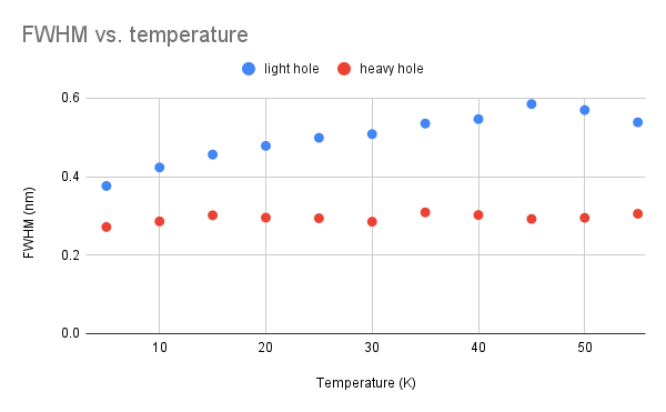
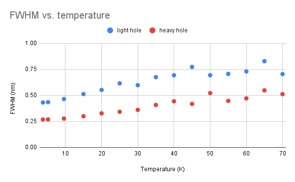
We generally see an upward trend, except for the FWHM of the heavy hole from the HeCd data, which appears not to change, so further investigations may be needed for that. The increase can be explained by phonon broadening. As temperature increases, there are more vibrations in the material, and phonons are particle representations of the vibrations. Phonons can interact with the electron-hole pairs that are created in photoluminescence, causing the peaks to widen.
Peak area
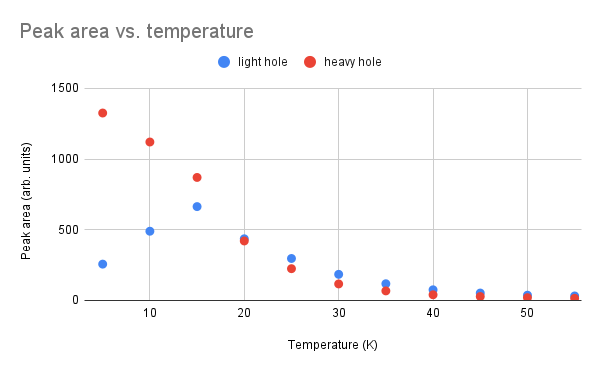
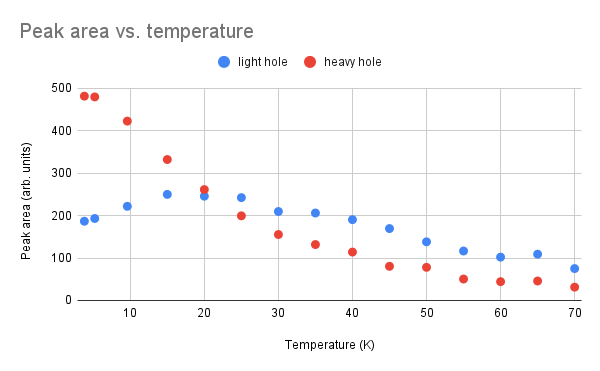
As temperature increases, the higher energy in the material opens up more nonradiative pathways, which is why there is a general decrease in intensity, which peak area represents. However, we see the light hole increases at the beginning. This is because the heavy hole pathway is a lower energy change, which makes it preferred, especially at lower temperatures. At higher temperatures, both pathways even out.
Conclusion
Most of these results can be explained, so I think our setup is ready for new projects. We have already replaced the GaAs quantum well with a Sb2O3 sample. We are trying to do Raman spectroscopy with the same setup up though we needed to change a few things. It is not working so far.
I finished my presentation, got advice for how to improve it, and gave a presentation to my research group at SJSU at our weekly group meeting. Next blog will be my last one, and I’ll write some concluding thoughts. See you then!
Citations
Chetvorno. Solid State Electronic Band Structure. 10 Mar. 2017, Wikimedia Commons, https://commons.wikimedia.org/wiki/File:Solid_state_electronic_band_structure.svg.
“Band Structure and Carrier Concentration of Gallium Arsenide (GaAs).” Www.ioffe.ru, www.ioffe.ru/SVA/NSM/Semicond/GaAs/bandstr.html.
Gammon, D., et al. “Phonon Broadening of Excitons in GaAs/AlxGa1−XAs Quantum Wells.” Physical Review B, vol. 51, no. 23, 15 June 1995, pp. 16785–16789, https://doi.org/10.1103/physrevb.51.16785.
Houng, M. P., et al. “Broadening Factor due to Electron–Phonon Collisions in Semiconductor Quantum Wells.” Journal of Applied Physics, vol. 77, no. 12, 15 June 1995, pp. 6338–6344, pubs.aip.org/aip/jap/article-abstract/77/12/6338/528048/Broadening-factor-due-to-electron-phonon, https://doi.org/10.1063/1.359104.
Jiang, Dapeng, et al. “Temperature Dependence of Photoluminescence from GaAs Single and Multiple Quantum‐Well Heterostructures Grown by Molecular‐Beam Epitaxy.” Journal of Applied Physics, vol. 64, no. 3, 1 Aug. 1988, pp. 1371–1377, https://doi.org/10.1063/1.341862.
Leave a Reply
You must be logged in to post a comment.